
Moore’s Law has guided semiconductor progress for more than half a century, with transistor scaling driving steady improvements in performance and efficiency. That pace is now slowing. To sustain momentum, the industry is turning to complementary technologies that create new opportunities for advancement. Erik Hosler, a semiconductor systems expert with a focus on lithography and architectural integration, points to photonics as one of the most promising directions shaping the future of chip design.
This shift reflects a broader change in how performance is pursued. Meeting growing demands for speed, efficiency, and system integration requires more than continued miniaturization. It depends on new approaches, and photonics is quickly becoming central to that effort.
Beyond Shrinking: Why Moore’s Law Needs a Broader Toolkit
Shrinking transistors has become exponentially more difficult. Fabrication at single-digit nanometer scales introduces quantum mechanical challenges, increases design complexity, and escalates production costs. Meanwhile, performance demands have not slowed. If anything, they have accelerated with the rise of artificial intelligence, edge computing, and connected systems.
Maintaining progress under these new constraints requires a broader approach. Rather than relying solely on physical scaling, the industry is now focused on architectural efficiency, smarter packaging, and the integration of novel technologies such as photonics and MEMS. It represents a diversification of the engineering playbook rather than a complete departure from Moore’s Law.
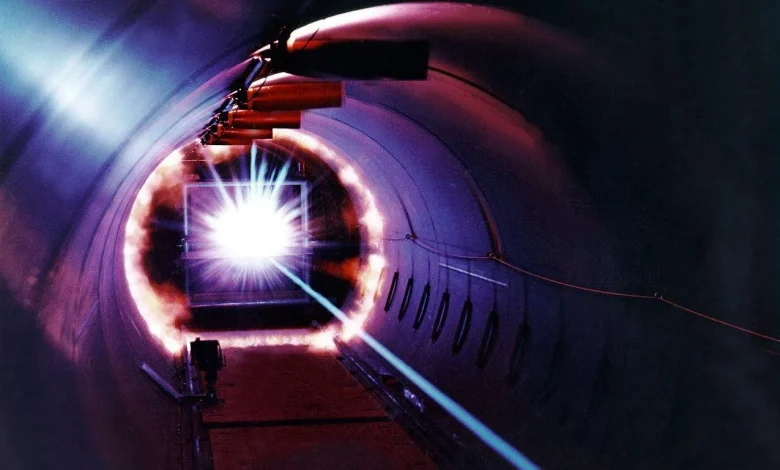
What Is Photonics and Why Does It Matter?
Photonics involves the generation, manipulation, and transmission of light, typically through lasers, waveguides, and optical fibers. In computing, its relevance lies in its ability to move data faster and more efficiently than traditional electrical interconnects.
As data volumes soar, bottlenecks arise not from processing speed but from communication between components. Electrical interconnects introduce resistance, heat, and latency. Photonics bypasses these limitations by transmitting signals as light, achieving higher bandwidth and lower power consumption over longer distances. That is why photonics is rapidly becoming a centerpiece of next-generation chip design.
Real-World Applications of Photonics
Photonics is already being deployed in data centers through fiber-optic networks and transceivers that facilitate high-speed data transfer between servers. More recently, chip-to-chip optical interconnects are emerging as a solution to bandwidth constraints in large-scale computing systems.
In research and advanced development, companies are exploring silicon photonics, which involves embedding optical components directly into CMOS-compatible substrates. This integration minimizes footprint and enables tighter coupling between logic and communication systems.
Photonics is not just for the cloud. It will soon be critical to AI inference engines, high-performance computing clusters, and even edge devices that require real-time processing with minimal latency.
The Thermal Advantage of Light
One of the most underappreciated benefits of photonics is its thermal efficiency. Electrical signaling generates heat through resistance. As more data is pushed across denser interconnects, thermal management becomes a limiting factor in chip design.
Light-based signaling eliminates this bottleneck. Optical signals do not suffer resistive losses, allowing systems to transmit massive volumes of data without incurring the same thermal penalty. It makes photonics particularly valuable in three-dimensional chip architectures and dense compute clusters, where managing heat is one of the biggest design challenges.
Challenges to Integration
Despite its promise, photonics integration into mainstream chip design faces significant challenges. Fabricating optical components with the precision and reliability of transistors is nontrivial. Waveguides, modulators, and detectors require more varied materials and manufacturing steps than traditional silicon circuits.
Integrating optics with electronics in the same package requires solving alignment, compatibility, and testing challenges that do not exist in pure electrical systems. However, investment and research into silicon photonics and advanced packaging are rapidly addressing these issues. Foundries are building processes specifically designed to support photonic elements. As a result, what was once experimental is becoming viable on a commercial scale.
Complementary Technologies and the Bigger Picture
Photonics does not act alone. Its value increases when used in combination with other technologies. MEMS devices, for instance, can adjust optical paths dynamically, enabling tunable filters, switches, and lenses. Advanced materials offer better light-handling capabilities and more stable performance across temperature variations.
This system-level thinking defines the new phase of semiconductor advancement. Instead of optimizing a single element, engineers are now tasked with integrating multiple domains to create emergent value. It reflects the essence of modern innovation, where system-level problems are solved by bringing together technologies that once operated in isolation.
Industry Reflections at SPIE
This vital perspective was captured during the SPIE Advanced Lithography symposium, where leaders across domains emphasized the importance of expanding the technological toolkit. Erik Hosler explains,
“Finally, the solution to keeping Moore’s Law going may entail incorporating photonics, MEMS, and other new technologies into the toolkit.”
His insight reflects an understanding shared by many in the industry. Continued progress no longer hinges on transistor size alone. It depends on how effectively diverse technologies are brought together to build high-performance, cost-efficient systems.
Photonics and AI: A Natural Pairing
Artificial intelligence is one of the key drivers of current semiconductor demand. AI workloads involve massive amounts of data transfer between processing units, memory, and storage, and traditional interconnects are increasingly unable to keep up.
Photonics offers a compelling solution. Optical interconnects can maintain the bandwidth required for AI training and inference without the power burden of electrical wires. It makes them ideal for scaling AI architectures across servers, chiplets, or even cores within a single package. As AI grows more complex, photonics will become not only advantageous but necessary.
Educating for a Photon-Based Future
Embracing photonics requires more than new hardware. It requires a new generation of engineers who are comfortable with optical, electrical, and materials design simultaneously. Educational institutions are beginning to offer interdisciplinary programs that train students to design hybrid systems.
The semiconductor workforce of the future will need to understand wavelength, impedance, fabrication chemistry, and mechanical tolerances simultaneously. This complexity is a challenge, but it is also a sign of the field’s maturity and potential. The barriers to photonics integration are technical, but the solutions are deeply human.
Lighting the Way Forward
Photonics is not a magic fix for Moore’s Law’s challenges. But it is one of the most promising tools for expanding what chips can do without relying on further transistor scaling.
By transmitting data more quickly, generating less heat, and enabling denser integration, photonics help redefine the meaning of performance. It moves the industry toward systems that are faster, more intelligent, and more efficient, not just smaller ones.